
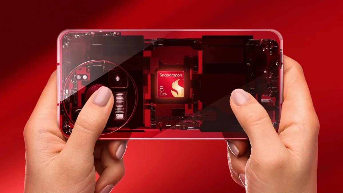
Even as the mobile industry continues to digest and benchmark the newly launched Snapdragon 8 Elite Gen 6 series, early intelligence regarding Qualcomm’s subsequent flagship mobile platform has already begun to surface within the semiconductor supply chain. According to preliminary reports originating from industry insiders and leaks tracking major foundry output, the San Diego-based chipmaker is actively developing its next-generation system-on-chip (SoC) under the internal codename "Honu." The upcoming architecture is projected to push single-core clock speeds to an unprecedented 5.4 GHz. However, despite the aggressive frequency targets, early performance simulations suggest that generational gains in benchmark outputs may see a relatively modest trajectory compared to its immediate predecessor.
The rumored platform, tentatively anticipated to debut commercially under a moniker such as the Snapdragon 8 Elite Extreme Gen 7—cataloged internally under the part number SM8A75—is widely expected to rely on Taiwan Semiconductor Manufacturing Company’s (TSMC) advanced 2nm N2P fabrication node. By sticking with a 2nm-class process node rather than migrating to a denser or entirely new process node right away, Qualcomm appears to be prioritizing architectural optimization, thermal efficiency, and manufacturing cost stabilization. Nonetheless, navigating the engineering hurdles of scaling performance to 5.4 GHz without triggering catastrophic thermal throttling remains a central focus for the company’s silicon design teams.
Main Facts and Technical Projections of the Honu Architecture
The core engineering objective behind the Honu project centers on maximizing single-threaded execution speed. Industry leaks indicate that Qualcomm is aiming for a sustained operating frequency window between 5.3 GHz and 5.4 GHz for its primary performance cores. Achieving this threshold typically demands substantial electrical current and introduces significant heat dissipation challenges in constrained smartphone chassis. However, early engineering samples suggest that Qualcomm has engineered the microarchitecture to maintain single-core power consumption levels roughly comparable to those observed in the Snapdragon 8 Elite Extreme Gen 6, which operates at a baseline clock speed of 5.0 GHz.
Despite the higher frequency ceiling, initial performance projections point toward a single-core score increase of less than 10 percent on standardized evaluation suites like Geekbench 6. This marginal efficiency gain per generational leap indicates that the industry is encountering diminishing returns when relying solely on clock speed increases within strict mobile thermal envelopes. Furthermore, comprehensive data regarding multi-core performance metrics, sustained load handling under extended gaming sessions, and the thermal design power (TDP) draw of the entire multi-cluster configuration remains undisclosed.
Evolution of Qualcomm’s Flagship Silicon Strategy
To understand the positioning of the Honu project, it is necessary to examine the rapid evolution of Qualcomm’s mobile platforms over recent cycles. Historically, mobile processors advanced through predictable iterations of node transitions and incremental core count adjustments. However, the introduction of custom Oryon CPU cores marked a strategic pivot for Qualcomm toward high-performance computing architectures capable of rivaling desktop counterparts in specific workloads.
Chronologically, the industry has transitioned from standard multi-cluster ARM-based designs to deeply integrated, high-frequency custom cores. The debut of the Snapdragon 8 Elite series established a new benchmark for flagship Android performance, emphasizing high-frequency operation and advanced neural processing capabilities. As Qualcomm rolled out successive iterations—culminating recently in the Gen 6 series—the focus expanded to include deeply integrated audio enhancements, such as the Snapdragon Sound Elite Gen 2 platform featuring doubled AI processing capabilities, and pervasive on-device machine learning operations.
The transition to the Honu architecture represents the next logical step in this timeline. By maintaining the N2P fabrication node, Qualcomm aligns its production roadmap with TSMC’s manufacturing milestones. TSMC’s N2P node is an optimized version of its base 2nm technology, offering enhanced performance and power efficiency characteristics over the initial N2 node variants. This strategic choice allows Qualcomm to leverage a mature or maturing high-end node while TSMC gradually redirects its cutting-edge capacity toward emerging 1.4nm nodes for future computing architectures.

Manufacturing Realities and Supply Chain Dynamics
The decision to utilize TSMC’s N2P fabrication process for the Honu platform highlights a broader economic and logistical reality facing the semiconductor industry: the escalating cost of leading-edge silicon manufacturing. Transitioning to smaller nodes—such as sub-2nm or 1.4nm thresholds—requires astronomical capital expenditure in lithography equipment, specifically Extreme Ultraviolet (EUV) systems. By utilizing an iterated 2nm process, Qualcomm can potentially manage wafer costs more effectively, shielding original equipment manufacturers (OEMs) and ultimately consumers from severe price hikes.
From a supply chain perspective, TSMC remains the primary foundry partner for Qualcomm’s top-tier Snapdragon lineup. The Taiwanese foundry’s capacity allocation plays a critical role in determining the release timeline and volume availability of flagship Android smartphones each year. Rumors surrounding the Honu chip suggest that Qualcomm is working closely with TSMC to ensure yield stability before locking in mass production schedules. Yet, because these details stem from preliminary supply chain tracking, the final commercial specifications, official marketing names, and definitive launch windows remain entirely unconfirmed by Qualcomm executives.
Analysis of Broader Market Implications
The emergence of details concerning the Honu SoC carries several critical implications for the broader mobile ecosystem. First, it underscores a shifting paradigm in mobile chipset marketing. For years, consumer tech marketing heavily emphasized raw clock speed milestones—breaking the 3 GHz barrier, then 4 GHz, and now approaching 5.4 GHz. However, as thermal limits in smartphones become increasingly restrictive, the practical utility of raw clock speed increases faces severe scrutiny.
If single-core performance increases by less than 10 percent despite a jump to 5.4 GHz, consumers and reviewers may question the tangible benefits of upgrading between consecutive generations. Consequently, manufacturers are forced to pivot their value propositions toward specialized capabilities, such as advanced on-device generative AI acceleration, hardware-accelerated ray tracing in mobile gaming, enhanced power efficiency for extended battery life, and superior wireless connectivity standards.
Second, the competitive landscape between Qualcomm, MediaTek, and Apple continues to intensify. With MediaTek pushing aggressive multi-core architectures and Apple maintaining tight hardware-software integration through its custom A-series silicon, Qualcomm cannot rely solely on frequency scaling to maintain its market share in the premium Android tier. The architectural enhancements embedded within the Honu platform must deliver meaningful real-world fluidity and energy efficiency rather than merely chasing high numbers on synthetic benchmarks.
Official Stance and Industry Outlook
As is standard corporate practice regarding unannounced product roadmaps, Qualcomm has declined to comment on the rumors surrounding the Honu codename or the specifications of its potential Snapdragon 8 Elite Extreme Gen 7 platform. Industry analysts note that engineering samples typically undergo multiple revisions before a final commercial design is approved for mass production. Consequently, early benchmark projections and frequency targets are subject to change as thermal testing, software optimization, and silicon tuning progress through the developmental pipeline.
For the time being, the mobile ecosystem remains firmly focused on the real-world deployment and optimization of the recently released Snapdragon 8 Elite Gen 6 series and its accompanying ecosystem features. As further data points emerge from regulatory filings, code repositories, and supply chain manifests, a clearer picture of Qualcomm’s long-term silicon strategy will materialize, establishing whether the 5.4 GHz threshold will redefine high-end mobile computing performance or simply serve as an incremental stepping stone toward future architectural paradigms.